PC3 Coatings
Applications:
1
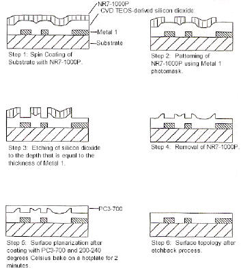
Planarizing Layer - etchback process to transfer planarity from
planarizing layer into
underlying dielectric. 2
Protective Coating - dicing and sawing operations to prevent
mechanical damage to the fabricated
device. 3
Adhesive Layer – attaching the device side of the wafer to a wafer
holder in back
grinding operations.
Properties: Superb planarizing capability.
Thickness range: 0.5-20 µm
Impact on productivity:

For Planarization Applications: Elimination of Chemical Mechanical Polishing
(CMP) in some applications.2 Suppression of
microloading effects in etchback process.
For Protective Coating Applications: Elimination of film peeling and
cracking during dicing operations.
For Adhesive Applications: 1
Easy removal in Resist Developer RD3 or RD6 after back
grinding and wafer separation. 2
Elimination of waxes from backside processing.
PC3 Coatings
Coating
Thickness
PC3-700 0.6µm - 1.6µm
PC3-1500
1.1µm - 3.2µm
PC3-6000 5.0µm - 12.2µm
|
Planarizing Coatings for
Sacrificial Etchback Applications |
|
Thickness Range |
0.7 - 12
µm |
|
Performance |
Superior planarizing
capability.
Outstanding etchback compatibility with underlying dielectric. |
|
Applications |
Surface planarization for planarization etchback process.
Protective coating.
Binding layer on the active side of devices for backgrinding.
Protective coating in wafer dicing. |
Development of novel UV
cross-linkable materials
for enhancing planarity
in via applications via
the correlation of
simulated and
experimental analyses
Beam Lead Quartz Chips
for Superconducting
Millimeter-Wave Circuits

If you don't find what you're looking for,
Contact Us.
We may have a suitable product that's not listed, or we may be
able to develop a material to fit your specific needs.
Tel : (02)2217-3442 / Fax : (02)2704-4070
|

