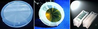
|
Gallium
Nitride Epi Wafers on Sapphire Substrates |
Novel Substrate
for Blue/UV LED
,
High Frequency MMIC, High Temperature
Electronic Production
GaN Epitaxial
Wafers are the ideal substrates for GaN homoepitaxial growth
and device manufacturing.

Substrate for III-V Nitrides Epitaxy. |
Applications
- New type
of substrate for GaN-based LEDs.
For more details, please click here.
- GaN
Epitaxial Wafers may be used as substrates for III-V
nitride epitaxial growth by MBE,
MOCVD and
CVD.
- No buffer
layer is required.
|
| Thickness of
GaN epilayer |
2 ~10 µm
|
| Wafer
diameter |
50 mm
|
| FWHM of
X-ray w-scan rocking curve |
<
600 arcsec
|
| Initial
substrate |
c-plane
sapphire |
| Orientation |
(0001)
|
| Structure |
wurtzite
|
| Conductivity |
n-type
|
| Surface |
as grown
|
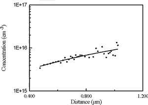
Depth profile for concentration Nd-Na
in GaN epitaxial layer
|
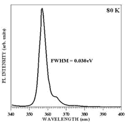 Photoluminescence spectrum
of GaN epitaxial layer |
|
|
Gallium
Nitride Epi Wafers On Sapphire Substrates
|
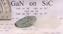
Gallium Nitride epi wafers
on SiC substrates |
Applications
- GaN
Epitaxial Wafers may be used as substrates for III-V
nitride epitaxial growth by MBE,
MOCVD and
CVD.
- No buffer
layer is required.
- GaN
Epitaxial Wafers are the ideal substrates for GaN
homoepitaxial growth and device manufacturing.
|
Technology
Gallium Nitride Epitaxial Wafer consists of a thin undoped GaN
epitaxial layer grown by hydride vapor phase epitaxy (HVPE)
directly on (0001)Si face on-axis 6H-SiC or 4H-SiC substrate.
|
Thickness of
GaN epilayer |
0.1 ~0.3 µm
|
| Diameter |
50 mm
|
| Substrate |
(0001) on
axis 6H-SiC or 4H-SiC |
| Orientation |
(0001)
|
| Structure |
wurtzite
|
| FWHM of
X-ray w-scan rocking curve |
<
250 arcsec
|
| Nd
?Na concentration |
1017
~1018 cm-3 |
| Surface |
as grown
|
Additional Information
- GaN layers and
SiC substrates are electrically conducting. Silicon carbide
insures excellent heat removal from nitride device
structure, which is important for high-power devices. GaN/SiC
wafers may be cleaved providing mirror-like facets for
nitride laser diodes.
- GaN layers
could be grown on SiC substrates supplied by customers.
|
|
Aluminum Nitride Epi
Wafers on Sapphire Substrates |
Aluminum Nitride Thin Layers for III-V Nitride Epitaxy
and
High Frequency Applications |
Applications
- AlN
Epitaxial Wafers may be used as substrates for
III-Nitrides epitaxial growth by MBE,
MOCVD and CVD
- AlN layers
have good insulation properties for fabrication of
Nitride-based FET structures.
- Good
piezoelectric properties of AlN make our layers an
excellent base for Surface Acoustic Wave devices.
|
|
Thickness of AlN epilayer |
0.1 ~0.3
mm |
| Diameter |
50 mm |
|
Substrate |
c-plane
sapphire |
|
Orientation |
(0001) |
|
Structure |
wurtzite |
|
Conductivity |
insulating |
| Surface |
as
grown |
|
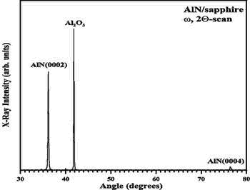
XRD spectrum (w, 2Q) for thin AlN layer grown on
sapphire |
|
|
Aluminum Nitride Epi
Wafers on SiC Substrates |
Aluminum Nitride Thin Layers for Nitrides Epitaxy
and High Frequency Applications |
Applications
- AlN
Epitaxial Wafers may be used as substrates for
III-Nitrides epitaxial growth by MBE,
MOCVD and CVD
- AlN layers
have good insulation properties for fabrication of
Nitride-based FET structures.
- Good
piezoelectric properties of AlN make our layers an
excellent base for Surface Acoustic Wave devices.
|
|
Thickness of
AlN epilayer |
0.1 ~0.2 µm
|
| Diameter |
50 mm
|
| Substrate |
(0001) on-
or off-axis 6H-SiC |
| Orientation |
(0001) on- &
off-axis |
| Structure |
wurtzite
|
| Conductivity |
insulating
|
| Surface |
as grown
|
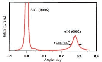
X-ray rocking curve (?-scan) from AlN/SiC
|
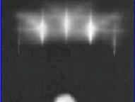
RHEED pattern image from AlN/SiC |
|