|
One of the biggest hurdles
to the widespread adoption of optical backplanes is the need for
an economic process to manufacture optical waveguides in
backplanes up to 1 m in size. Groups in Japan, Europe and N.
America have been investigating a number of techniques for
fabricating optical waveguides embedded within conventional
PCBs. PPC/Isola use silica as their optical waveguide which has
the benefit of very low loss, but is difficult to fabricate.
STET use polymer, and emboss the waveguides. It is difficult to
achieve good surface finish using this process, and the
resultant guides can have high losses.
BPA identify polymer as
being attractive for a number of reasons including its intrinsic
low cost and scalability. BPA highlight concerns of as high loss
(0.1 – 0.6 dB/cm) and insufficiently resistant to lamination and
reflow processes used in PCB manufacture. Terahertz Photonics
set out to develop its photosensitive TRUEMODE TM polymer
to simultaneously meet these requirements.
The resultant TRUEMODE
BackplaneTM
polymer has:
• Optical loss of < 0.04 dB/cm at 850
nm
• A high glass transition temperature
of 150°C.
• A high degradation temperature of 350 °C
Terahertz Photonics come
to the optical backplane world with a growing heritage in
polymer optical components. Variants of the TRUEMODETM family of
polymers are finding application in components including
splitters and fan-outs. Expertise obtained in the tight
fabrication tolerances and polymer requirements for these single
mode components fed naturally into the development of TRUEMODETM
polymer for optical backplanes.
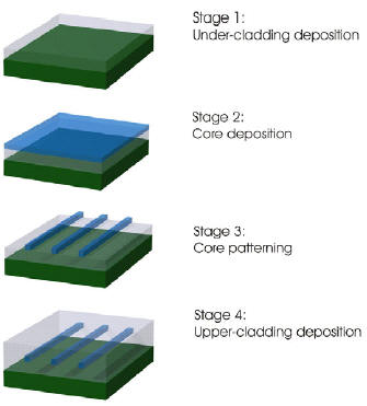
The process by which the
optical medium is deposited 0on the substrate and patterned to
form waveguides is central to optical backplanes. The process
consists of four stages. See figure
3.

Figure 3: TRUEMODE
BackplaneTM
process
The first
stage consists of deposition of monomers in a ~20 μm
thick undercladding using screen printing followed by low
intensity UV polymerisation.
The second
stage consists of the deposition of a 50 μm
thick layer of monomers having a refractive index typically 1%
higher than the cladding.
In the third
stage the polymer is patterned by photolithography or laser
direct write using a low power UV laser such as a He:Cd laser
[2].
The final
stage is a repeat of the first, though the layer thickness may
be increased for greater protection of the core.
If you don't find what you're looking for,
Contact Us.
We may have a suitable product that's not listed, or we may be
able to develop a material to fit your specific needs.
Tel : (02)2217-3442 / Fax : (02)2704-4070
|
|

