廠商登入區員工登入區學術研究機構登入區    
  製品介紹 ・サービス

Si (111)


Si ( 001)


 返回首頁 > 產品與技術 > 碳化矽晶圓
 
 
The improvements made in SiC semiconductor device technology for electronic and optoelectronic applications are due in part to the commercial availability of Sic substrates of ever-increasing diameter and quality. Examples of current state-of-the-art devices include: high brightness and ultra-bright blue and green InGaN-based LEDs which take full advantage of the electrical conductivity of the 6H-SiC substrate by employing a conductive AlGaN buffer layer; microwave MESFETs on semi-insulating 4H-SiC substrates with power densities as high as 4.6 W/mm at 3.5 GHz and total CW output power of 100 W at 2.0 GHz from a single chip; 20 kV and 25 A p-i-n diodes fabricated on high quality Sic epitaxial layers; 1 cm2 thyristors conducting 300 A at 5.5 V with 1770 V blocking voltage; and GaN/AlGaN HEMTs fabricated on semi-insulating 4H-SiC substrates exhibiting power densities of 11.4 W/mm at 10 GHz. These exciting device results stem primarily from the exploitation of the unique electrical and thermophysical properties offered by SiC compared to Si and GaAs. Among these are: a large band gap for high temperature operation and radiation resistance, high critical breakdown field for high power output, high saturated electron velocity for high frequency operation, and significantly higher thermal conductivity for thermal management of high power devices.

XBH supplies high quality SiC epi-ready substrates with both production and research grades

3" 4H N-Type SiC Epi-ready Substrates
3” 4H Semi-Insulating SiC Epi-ready Substrate
2” 4H N-Type SiC Epi-ready Substrate
2” 6H Semi-Insulating SiC Epi-ready Substrate
2” 6H N-Type SiC Epi-ready Substrate
Wafer Diameter :  34.9 ± 0.25 mm   50.8 ± 0.25 mm
Edge Exclusion :
 <5 mm (for 50.8 mm diameter)
Wafer Thickness : 300 ± 25 µm
Micropipe Density :
<100 cm-2
Etch Pit Density (on Si face) : 
<104 cm-2
Dopant : Nitrogen
Net Dopant Concentration :
1-3 x 1018 cm-3
Conductivity : n-type
Resistivity : 0.04 ohm cm ± factor of 2
Surface Finish : Si face polished
Polytype Homogeneity :
>95%
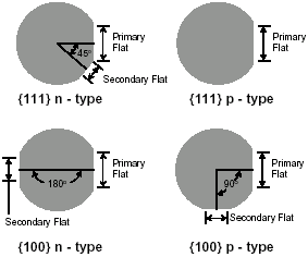
Orientation : On-axis:
<0001>  ± 0.5°
                       Off-axis:
<0001> 8° off towards <1100> or <1120>
Crystal Structure : Hexagonal
Bandgap : 3.2 eV
Thermal Conductivity :
4.9 Wcm-1 K-1
Mohs Hardness : ~9.5


If you don't find what you're looking for, Contact Us. We may have a suitable product that's not listed, or we may be able to develop a material to fit your specific needs. Tel : (02)2217-3442 / Fax : (02)2704-4070


  Copyright and Disclaimerc © David Lu & Corp.