This technology deposits electronic materials onto low-temperature,non-conformal
substrates without masks or resists.
A neglected middle ground exists in microelectronic fabrication.
Major manufacturing techniques are designed to deposit very small
electronic features and relatively large ones. But no deposition
technology currently on the market is aimed at crucial midsize
components such as resistors, capacitors and inductors. However, a
new technology for producing midsize electronic features has
recently been developed. Without masks or resists, this technology
can write lines of electronic materials less than 25 μm wide onto
polymer, glass or ceramic substrates, for manufacturing of printed
wiring boards (PWBs) and other devices.

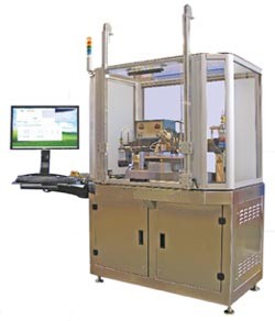
Sol Jet
printer
is a valuable tool for product development because it
generates circuitry on PCBs directly from a CAD file.
Sol Jet
printer
makes it much easier to implement and validate design changes
without the need for legacy mask sets and other accessories
required by conventional deposition techniques. The
elimination of masks and resists also permits on-the-fly
changes and rapid design iterations. The result is faster
time-to-market for new products.
Sol Jet
printer
微線路圖形印刷,低溫接著塗佈機,不使用光罩,節省成本,改善生產效率
Sol Jet
printer
提供噴墨製程厚膜生產,彈性圖形設計加快生產效率
 |
 |
|
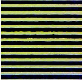
10
μm line width
20
μm pitch
Enables
>36,000
spots/hour |
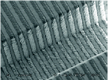
Conformal
deposition over varying topologies with no change in Z
height}
60
μm line width
500
μm
trenches |
Direct Printing of Circuit Boards Using
Aerosol Jet
Optimizing Aerosol Jet® Printing Of Silver
Interconnects On Polyimide Film For Embedded Electronics
Applications
Photo resist printing
... contact to the printhead nozzle
plate results
in higher jetting stability and longer printhead lifetime
If you don't find what you're looking for,
Contact Us.
We may have a suitable product that's not listed, or we may be
able to develop a material to fit your specific needs.
Tel : (02)2217-3442 / Fax : (02)2704-4070
|
|

